Paolo Gargini
Paolo Gargini
Contact Menu
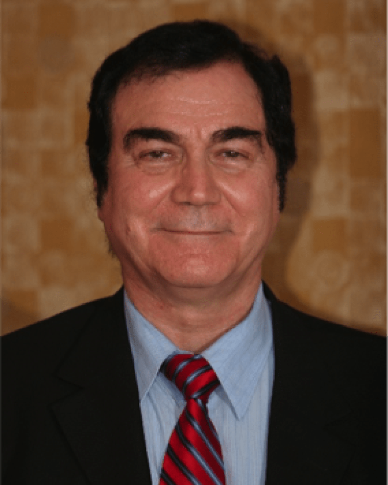
At the end of 2012 Dr. Paolo Gargini returned to the world of research (e.g., ITRS, IEUVI, ICCI, Stanford University, UC Berkeley and other organizations) after having worked for 34 years at Intel Corporation. During his tenure at Intel, Dr. Gargini was Director of Technology Strategy in Santa Clara, California. While at Intel, Dr. Gargini was also responsible for worldwide research activities conducted by universities and consortia for the benefit of the Technology and Manufacturing Group. Dr. Gargini was born in Florence, Italy and received a doctorate in Electrical Engineering in 1970 and a doctorate in Physics in 1975 from the Università di Bologna, Italy, both with full honor and marks. He has done research at Stanford Electronics Laboratory, and Fairchild Camera and Instrument Research and Development in Palo Alto from 1970 to 1977. Since joining Intel in 1978 he was responsible for developing the building blocks of HMOS III and CHMOS III technologies used in the 1980s for the 80286 and the 80386 processors. In 1985 he headed the first submicron process development team at Intel. In 1995, Dr. Gargini was elevated to Intel Fellow. Dr. Gargini has been the Chairman of the Executive Steering Council (ESC) of I300I and, subsequently, of International Sematech from 1996 to 2000. He was then a member of the Sematech Board until 2012. Since 1998, Dr. Gargini has been the Chairman of the International Technology Roadmap for Semiconductors (ITRS). Since 2016 he is the Chairman of IRDS. He also heads the International EUV Initiative (IEUVI) and the International Consortia Cooperation Initiative (ICCI). Dr. Gargini became the first Chairman of the Governing Council of the Nanoelectronics Research Initiative (NRI) funded in June 2005 by SIA. Dr. Gargini was inducted in the VLSI Research Hall of Fame in 2009. Dr. Gargini was elevated to International Fellow of the Japan Society of Applied Physics in 2014.
-
Special SessionPresenterDateSeriesASC 2018Presentation CategorySpecial Session: Superconductor Electronics Technology Roadmap

